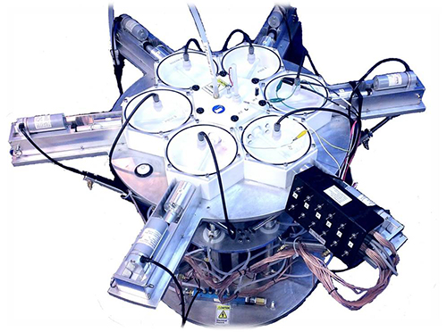
Electrochemical Atomic Layer Deposition System (eALD)
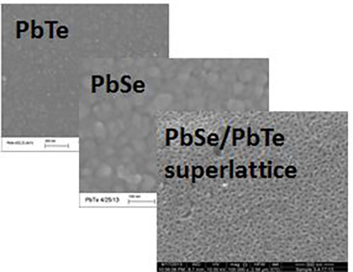
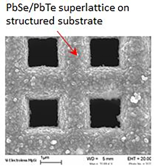
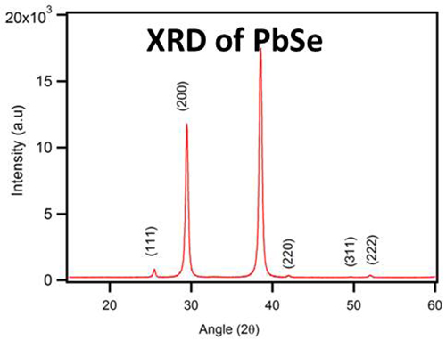
The wafer-scale automated electrochemical Atomic Layer Deposition (eALD) system is an ideal tool to grow nanomaterials atomic layer by atomic layer by using surface limited chemical reactions (the phenomenon also known as an under potential deposition). Although similar to certain degree to more common vacuum Atomic Layer Deposition technique, eALD offers a number of unique advantages particularly for deposition of superlattices (for a nonlimiting example, PbTe/PbSe or Bi2Te3/Sb2Te3), where such superlattices can be grown at a single temperature quickly, while classical ALD due to different temperatures of depositions of individual materials require temperature adjustment of the system, resulting in lengthy and not very practical process.
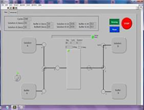
In eALD, atomic monolayers are formed on the surface during exposure to the proper solution and potential. Between different deposition cycles the surface of the substrate is exposed to the buffer solution that is used to remove the non-specifically bound species from the surface. By repeating these cycles the designed nanomaterial can be formed.
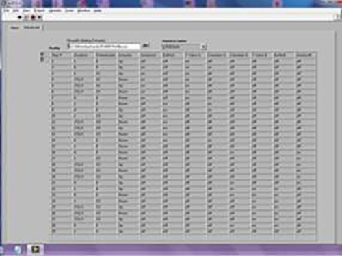
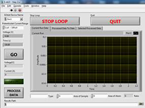
To provide uniform and good quality nanomaterials and nanostructures MicroXact developed an automated tool that has the following unique features:
Features
- Uniform wafer-scale coating of wide range of materials and structures (up to 150mm wafers were coated to date)
- Fast cycle time (fast electrolyte exchange)
- Minimized cross-contamination of solutions
- Minimized solution consumption (minimized solution waste)
- Temperature control
- Multiple solutions can be used without exposing the surface of the sample to air (up to 5 different solutions and buffer)
- Automation software for unattended operation with capability to in-situ adjust deposition parameters